- 您现在的位置:买卖IC网 > Sheet目录516 > SIS902DN-T1-GE3 (Vishay Siliconix)MOSFET N-CH D-S 75V 1212-8 PPAK
�� ��
��
��SiS902DN�
�Vishay� Siliconix�
�Dual� N-Channel� 75-V� (D-S)� MOSFET�
�PRODUCT� SUMMARY�
�FEATURES�
�V� DS� (V)�
�75�
�R� DS(on)� (� Ω� )�
�0.186� at� V� GS� =� 10� V�
�0.228� at� V� GS� =� 4.5� V�
�I� D� (A)�
�4� e�
�4� e�
�Q� g� (Typ.)�
�2.1� nC�
�?� Halogen-free� According� to� IEC� 61249-2-21�
�Definition�
�?� TrenchFET� ?� Power� MOSFET�
�?� Low� Thermal� Resistance� PowerPAK� ?�
�Package� with� Small� Size� and� Low� 1.07� mm�
�Profile�
�?� 100� %� R� g� Tested�
�?� 100� %� UIS� Tested�
�?� Compliant� to� RoHS� Directive� 2002/95/EC�
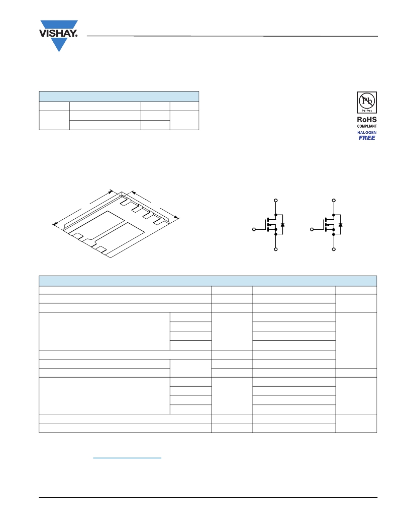
�PowerPAK� 1212-8�
�APPLICATIONS�
�?� POL�
�D� 1�
�D� 2�
�3.30� mm�
�1�
�S1�
�G1�
�3.30� mm�
�2�
�3�
�S2�
�G2�
�8�
�D1�
�D1�
�4�
�G� 1�
�G� 2�
�7�
�6�
�D2�
�5�
�D2�
�Bottom� View�
�S� 1�
�S� 2�
�Ordering� Information:� SiS902DN-T1-GE3� (Lead� (Pb)-free� and� Halogen-free)�
�N-Channel� MOSFET�
�N-Channel� MOSFET�
�ABSOLUTE� MAXIMUM� RATINGS� T� A� =� 25� °C,� unless� otherwise� noted�
�Parameter�
�Drain-Source� Voltage�
�Gate-Source� Voltage�
�T� C� =� 25� °C�
�Symbol�
�V� DS�
�V� GS�
�Limit�
�75�
�±� 20�
�4� e�
�Unit�
�V�
�Continuous� Drain� Current� (T� J� =� 150� °C)�
�Pulsed� Drain� Current�
�Avalanche� Current�
�Single-Pulse� Avalanche� Energy�
�T� C� =� 70� °C�
�T� A� =� 25� °C�
�T� A� =� 70� °C�
�L� =� 0.1� mH�
�I� D�
�I� DM�
�I� AS�
�E� AS�
�4� e�
�3� a,� b�
�2.4� a,� b�
�8�
�2�
�0.2�
�A�
�mJ�
�T� C� =� 25� °C�
�15.4�
�Maximum� Power� Dissipation�
�T� C� =� 70� °C�
�T� A� =� 25� °C�
�P� D�
�9.9�
�3.1� a,� b�
�W�
�T� A� =� 70� °C�
�2� a,� b�
�Operating� Junction� and� Storage� Temperature� Range�
�Soldering� Recommendations� (Peak� Temperature)� c,� d�
�T� J� ,� T� stg�
�-� 55� to� 150�
�260�
�°C�
�Notes:�
�a.� Surface� Mounted� on� 1"� x� 1"� FR4� board.�
�b.� t� =� 10� s.�
�c.� See� Solder� Profile� (� www.vishay.com/ppg?73257� ).� The� PowerPAK� 1212-8� is� a� leadless� package.� The� end� of� the� lead� terminal� is� exposed�
�copper� (not� plated)� as� a� result� of� the� singulation� process� in� manufacturing.� A� solder� fillet� at� the� exposed� copper� tip� cannot� be� guaranteed� and�
�is� not� required� to� ensure� adequate� bottom� side� solder� interconnection.�
�d.� Rework� Conditions:� manual� soldering� with� a� soldering� iron� is� not� recommended� for� leadless� components.�
�e.� Package� limited.�
�Document� Number:� 64804�
�S09-0661-Rev.� A,� 20-Apr-09�
�www.vishay.com�
�1�
�发布紧急采购,3分钟左右您将得到回复。
相关PDF资料
SISA10DN-T1-GE3
MOSFET N-CH 30V 30A 1212-8
SIZ700DT-T1-GE3
MOSFET N-CH D-S 20V PPAK 1212-8
SIZ710DT-T1-GE3
MOSFET N-CH D-S 20V POWERPAIR
SIZ720DT-T1-GE3
MOSFET N-CH D-S 20V POWERPAIR
SIZ902DT-T1-GE3
MOSFET N-CH 30V DUAL D-S
SKY12322-86LF-EVB
BOARD EVALUATION FOR SKY12322-86
SKY12323-303LF-EVB
BOARD EVALUATION FOR SKY1232-303
SKY12324-73LF-EVB
BOARD EVALUATION FOR SKY12324-73
相关代理商/技术参数
SISA04DN
制造商:VISHAY 制造商全称:Vishay Siliconix 功能描述:N-Channel 30 V (D-S) MOSFET
SISA04DN-T1-GE3
功能描述:MOSFET 30V 2.15mOhm@10V 40A N-Ch G-IV
RoHS:否 制造商:STMicroelectronics 晶体管极性:N-Channel 汲极/源极击穿电压:650 V 闸/源击穿电压:25 V 漏极连续电流:130 A 电阻汲极/源极 RDS(导通):0.014 Ohms 配置:Single 最大工作温度: 安装风格:Through Hole 封装 / 箱体:Max247 封装:Tube
SISA10DN
制造商:VISHAY 制造商全称:Vishay Siliconix 功能描述:N-Channel 30 V (D-S) MOSFET
SISA10DN-T1-GE3
功能描述:MOSFET 30V 3.7mOhm@10V 30A N-Ch G-IV
RoHS:否 制造商:STMicroelectronics 晶体管极性:N-Channel 汲极/源极击穿电压:650 V 闸/源击穿电压:25 V 漏极连续电流:130 A 电阻汲极/源极 RDS(导通):0.014 Ohms 配置:Single 最大工作温度: 安装风格:Through Hole 封装 / 箱体:Max247 封装:Tube
SISA12ADN-T1-GE3
功能描述:MOSFET 30V 4.3mOhm@10V 25A N-Ch
RoHS:否 制造商:STMicroelectronics 晶体管极性:N-Channel 汲极/源极击穿电压:650 V 闸/源击穿电压:25 V 漏极连续电流:130 A 电阻汲极/源极 RDS(导通):0.014 Ohms 配置:Single 最大工作温度: 安装风格:Through Hole 封装 / 箱体:Max247 封装:Tube
SISA12DN-T1-GE3
功能描述:MOSFET 30V 25A 28W 4.3mohm @ 10V
RoHS:否 制造商:STMicroelectronics 晶体管极性:N-Channel 汲极/源极击穿电压:650 V 闸/源击穿电压:25 V 漏极连续电流:130 A 电阻汲极/源极 RDS(导通):0.014 Ohms 配置:Single 最大工作温度: 安装风格:Through Hole 封装 / 箱体:Max247 封装:Tube
SISA14DN-T1-GE3
功能描述:MOSFET 30V 5.1mOhm@10V 14.1A N-Ch G-IV
RoHS:否 制造商:STMicroelectronics 晶体管极性:N-Channel 汲极/源极击穿电压:650 V 闸/源击穿电压:25 V 漏极连续电流:130 A 电阻汲极/源极 RDS(导通):0.014 Ohms 配置:Single 最大工作温度: 安装风格:Through Hole 封装 / 箱体:Max247 封装:Tube
SISA18ADN-T1-GE3
功能描述:MOSFET 30V 7.5mOhm@10V 18A N-Ch G-IV
RoHS:否 制造商:STMicroelectronics 晶体管极性:N-Channel 汲极/源极击穿电压:650 V 闸/源击穿电压:25 V 漏极连续电流:130 A 电阻汲极/源极 RDS(导通):0.014 Ohms 配置:Single 最大工作温度: 安装风格:Through Hole 封装 / 箱体:Max247 封装:Tube